Henkel Debuts 1 GW Scale Innovation Hub for India’s Electronics Sector
Henkel launches a Bengaluru innovation hub to localize electronics manufacturing, accelerating AI, 5G, and EV development under Make in India.
Localizing the Electronics Value Chain: New Facility to Accelerate "Make in India" for 5G, AI, and EV Markets
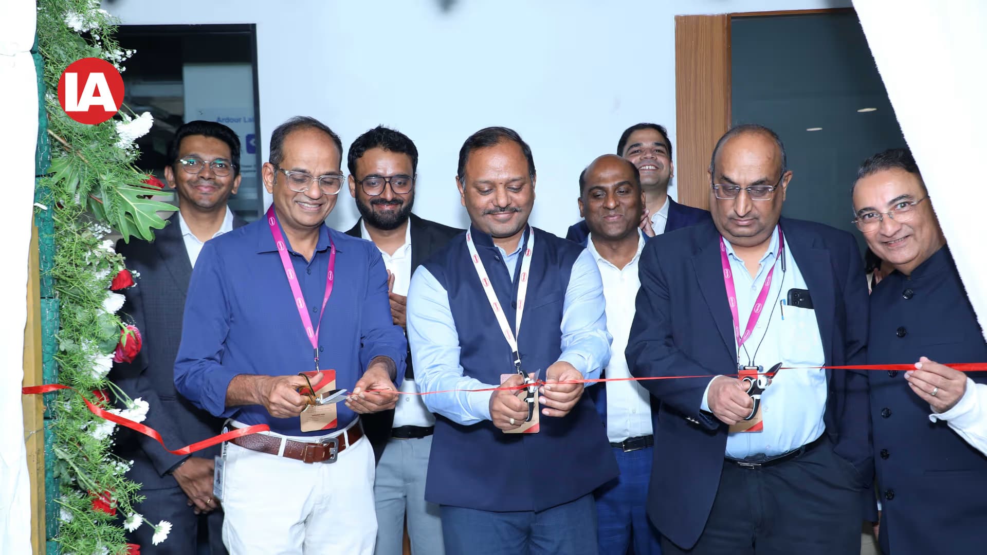
BENGALURU — March 2026 — Henkel has officially inaugurated its Customer Application Center in Bengaluru, a strategic move designed to anchor India’s rapidly maturing electronics manufacturing ecosystem. As the nation’s electronics output has surged six-fold over the last decade, this new co-innovation hub addresses a critical infrastructure gap: the need for localized, world-class validation and testing.
The 5,000 sq.ft facility allows manufacturers to develop, qualify, and scale advanced materials solutions—such as high-performance adhesives and thermal management systems—without the costly and time-consuming process of sending prototypes overseas.
Inside the Hub: Engineering for Precision
The facility is built to replicate real-world manufacturing environments, enabling "right-first-time" development for complex device architectures.
Laboratory Powerhouse: Nearly 2,400 sq.ft of dedicated lab space focused on advanced thermal management and precision dispensing.
High-Tech Investment: Over 60% of the total investment was directed toward advanced testing equipment and electrical characterization tools.
Rapid Prototyping: Features rapid-cure chambers and liquid cooling validation setups to compress the time-to-market for new hardware.
Strategic Focus on High-Growth Sectors
The center is designed to serve as the primary engineering partner for five key pillars of India’s digital and industrial economy:
| Sector | Application Focus |
| Telecom & 5G | Fiber network expansion and high-speed infrastructure coatings. |
| Data Centers & AI | Advanced thermal interface materials for high-density computing. |
| Power Electronics & EV | Battery management systems and EV charging station reliability. |
| Industrial Automation | Ruggedized adhesives for sensors and robotic controllers. |
| Medical Electronics | Bio-compatible protective coatings for advanced medical devices. |

Strengthening India's Electronics Future
By bringing process optimization and reliability validation onshore, Henkel is directly supporting the Production-Linked-Incentive (PLI) objectives of the Indian government.
"What manufacturers increasingly need is not just world-class materials, but a local partner who can co-develop and validate those materials under real production conditions. This center is our most tangible expression yet of Henkel’s long-term commitment to India’s electronics future."— S Sunil Kumar, Country President – India, Henkel.
FAQ.
Why was Bengaluru chosen for this facility?
Bengaluru is the heart of India's electronics R&D. By locating the center here, Henkel places its application expertise directly alongside semiconductor design firms, global OEM engineering teams, and the massive talent pool that defines India's "Silicon Valley."
How does this facility help "Make in India"?
Previously, many Indian manufacturers had to route material qualification and reliability testing through overseas labs in Europe or East Asia. This local hub allows these activities to happen onshore, significantly reducing development cycles and costs for domestic electronics brands.
What is "Co-Innovation" in this context?
Unlike a standard testing lab where samples are simply mailed in, the Co-Innovation model allows customer engineering teams to work side-by-side with Henkel experts. They can tweak material formulations and dispensing processes in real-time to fit specific device architectures.